6601期末必考点
1.光刻(Lithography)
三个主要过程:Coating $\rightarrow$ Expose $\rightarrow$ Developing
1.1 Light Intensity
Mercury Arc Lamp: V Light Wavelength大概在300-400nm之间时,也就是g-line、h-line、i-line光刻胶,用的是深汞灯(Hg lamp)进行光刻,光刻强度低(low intensity),因此所需曝光时间长。
Excimer laser Source(准分子激光源): 而当UV Light Wavelength下降到300以下时,就是KrF光刻胶,用的是Deep UV(DUV),也就是深紫外灯,其拥有更高的光刻强度(high intensity),则所需曝光时间就很短.
1.2 Resists
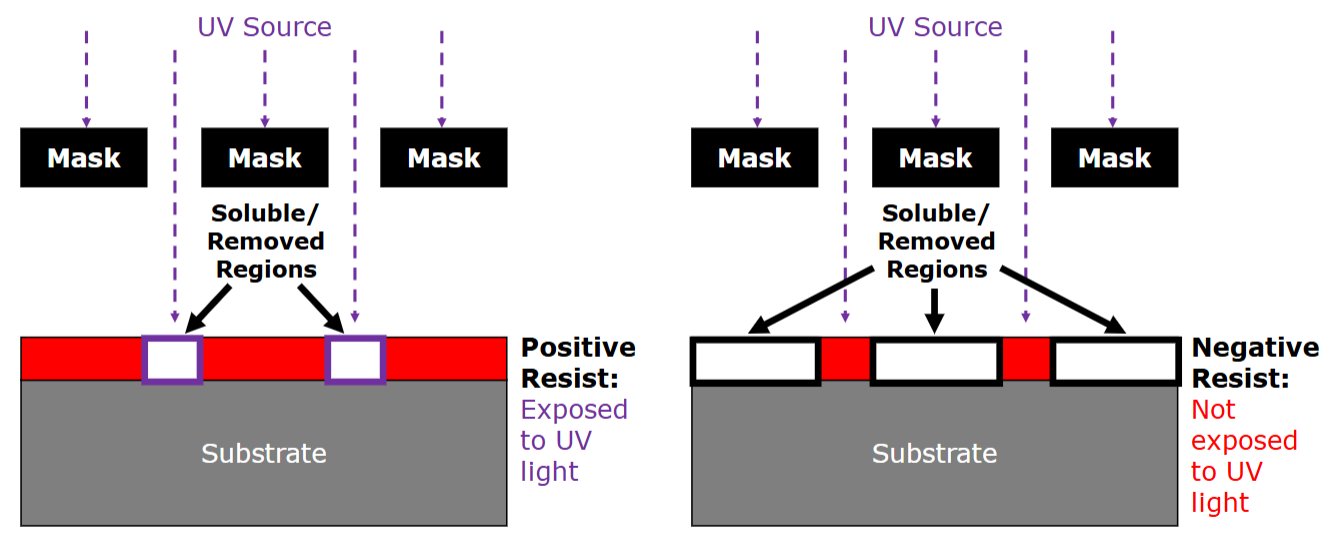
如上图所示,左边是正性光刻胶,被UV光照的地方溶解,而有掩膜(Mask)遮盖的地方,也就是没有光照的光刻胶不溶解;而右边则是负性光刻胶,其工作机理与正光刻胶相反,被光照的光刻胶不溶解,而被掩膜遮盖的位置则溶解。
1.3 Eight Steps of Lithography
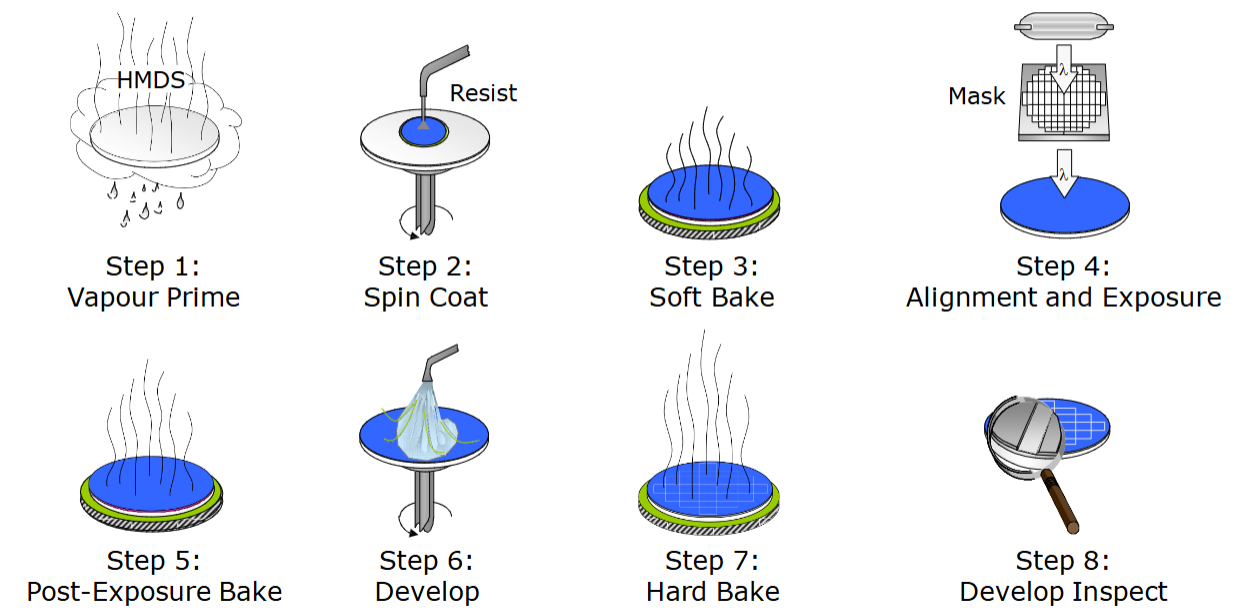
step 1: Vapour Prime
① Wafer dehydration bake;② HMDS adhesion clean and dry
step 2: Spin Coat
① Make PR to expected Thickness
另外,Resist layer thickness depends on the viscosity of resist and is inversely proportional to the square root of the spin speed, $t{\frac{\alpha}{\omega_2}}$.
Thinner Resist: ${I_R}\simeq{[\frac{viscosity\times{solid\,content}}{\sqrt{spin\,speed}}]}$,Spin speed越快越好,如果转速越慢,表面的光刻胶就会越厚。
step 3: Soft Bake
① Partial evaporation of resist solvents; ② Improves resist-to-wafer adhesion; ③ Improves etch resistance
短时间的Pre-bake可以防止由于残留在PR中的的solvent过多而导致的UV light reaching the PAC;
Over-bake则会增加sensitivity to UV light,甚至可能破坏PAC和减少solubility of the PR。
step 4: Alignment and Exposure
① Transfer pattern to wafer; ② Active PAC
step 5: Post-Exposure Bake
① Evaporate all solvnent
还能减少驻波(standing wave)效应的影响
step 6: Developing
① Remove the soluble portion with a solvent; ② Patterning
step 7: Hard Bake
① Evaporate solvnent from step6 adhesion; ② Etch resistance
step 8: Develop Inspect
① Check the quality of process to ensure the pattern is transfered.
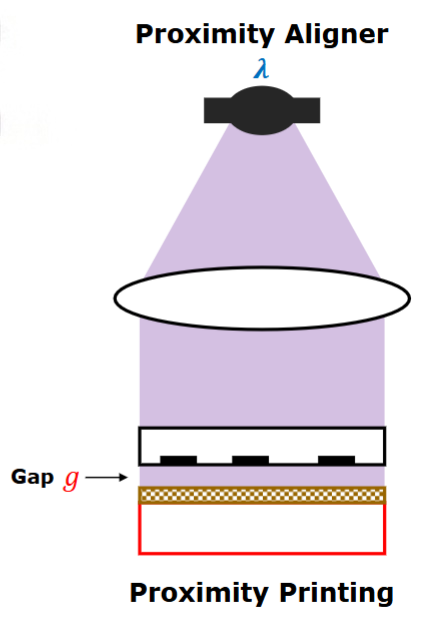
1.4 Printing
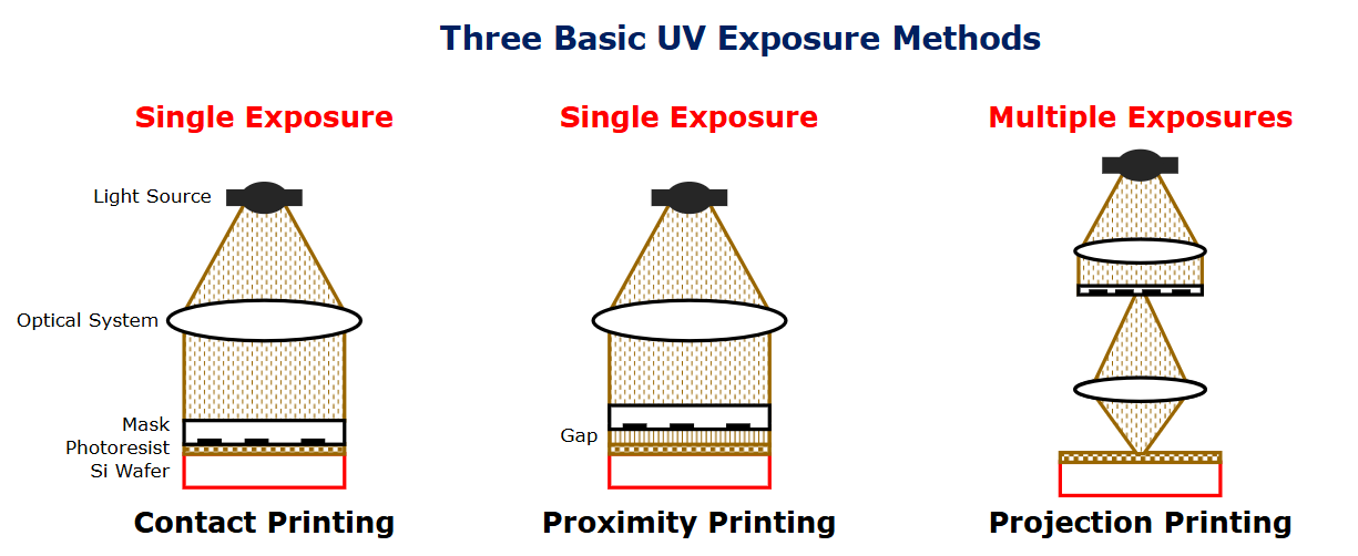
注意:在Contact Printing和Proximity Printing中,掩膜被称作mask,但是在Projection Printing中,则被成为reticle,但实际上两者是一样的。
另外,在Contact Printing中,mask和photoresist是直接接触的;而在Proximity Printing中,mask和wafer并没有直接接触,这一改动可以prevent dust particles。
1.5 Minimum Linewidth / Resolution
Resolution for the proximity printer:
$W_{min}\simeq{\sqrt{k_1\lambda{g}}}$ , $\lambda=\frac{c}{f}$, $E=h\frac{c}{f}$
$k_1$ is a constant
$\lambda$ is Wavelength of the exposure source
$g$ is Gap between the mask and the wafer surface
and more larger resolution is better.
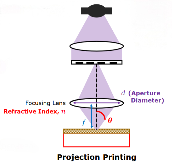
1.6 Numerical Aperture
NA is a measure of the ability to collect light
$NA=nsin\theta$
Where $n=$refraction index (the medium in which the system is immersed, in this $n=1$ for air)
So n is for air or water not for LENS.
$NA=sin\theta\,{\simeq}{\frac{\frac{d}{2}}{f}}={\frac{d}{2f}}$
1.7 Depth of Focus
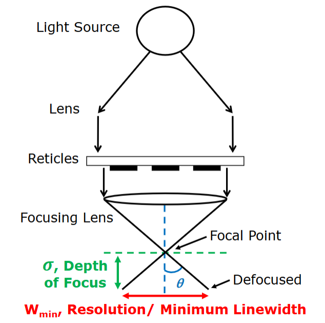
Depth of focus:
$\sigma=\pm{\frac{\frac{W_{min}}{2}}{tan\theta}}\simeq\pm{\frac{\frac{k\lambda}{2NA}}{sin\theta}}$
$\sigma=\pm{\frac{\frac{k\lambda}{2NA}}{\frac{NA}{n}}\simeq\pm{\frac{nk_2{\lambda}}{(NA)^2}}}$
$\lambda$越小或者$NA$越大,则$\sigma$越小;$\sigma$越小越好
1.8 光强度图
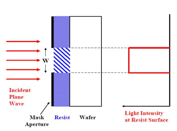
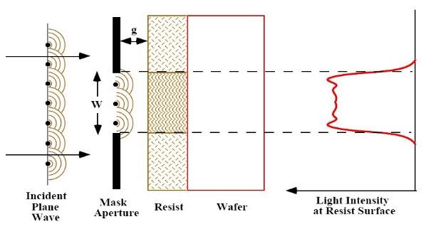
左边是Contact Printeing,右边是Proximity Printing。
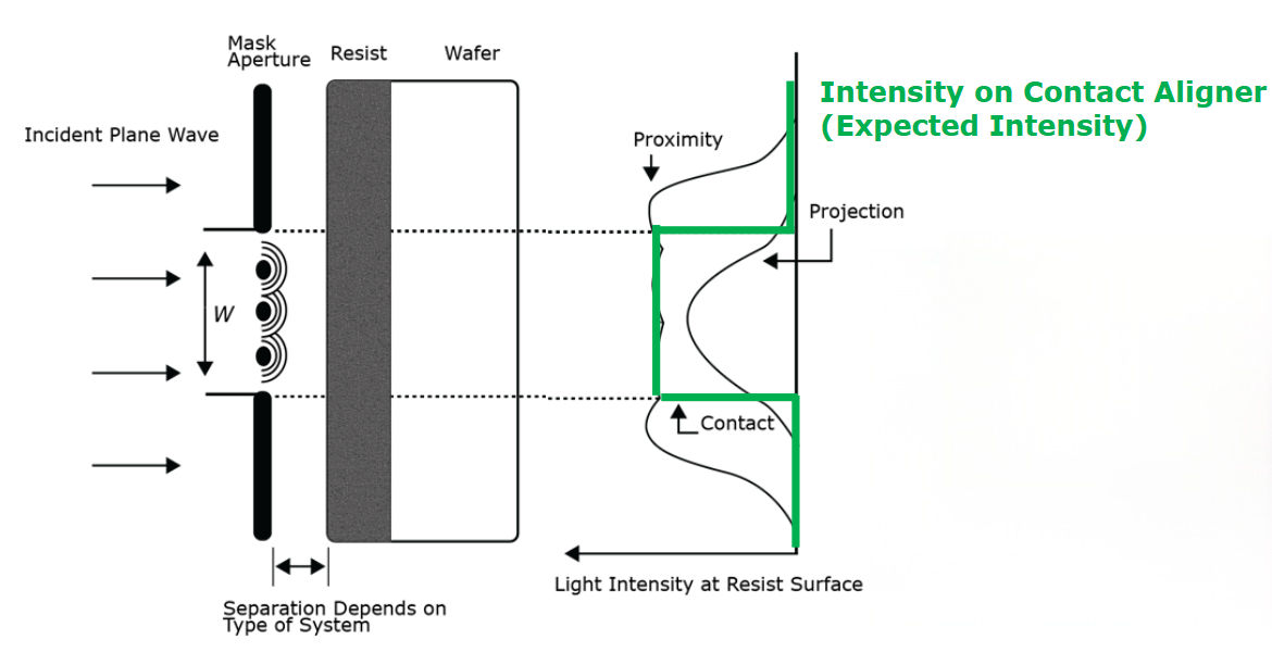
上面的光强度图要求要会画,三种光刻模式都要会。
1.9 Modulation transfer function (MTF)
We hope projection printer shows no diffraction, like contact printer light and dark edge is very sharp.
$MTF=\frac{I{max}-I{min}}{I{max}+I{min}}$,MTF is for optical system(Lens) and bigger the better.
2 光刻胶技术(resist technology)
2.1 Contrast curve
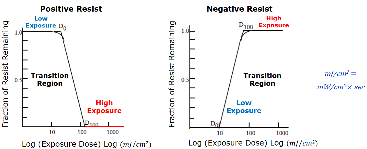
A good resist, Dose critical is 50,
You shine 51 dose, all resist is soluble;
You shine 49 dose, nothing happened.
一个重要的参数:
Sensitivity: $D_{100}(D_f)$
Chemical contrast $\gamma$ $\rightarrow$ slope of curve defined as:
$\gamma=\frac{1}{log{10}\frac{(D{100})}{D_{0}}}$
2.2 Critical Modulation transfer function (CMTF)
从上面的 $\gamma$ 可以推导出CMTF:
$CMTF=\frac{D_f-D_0}{D_f+D_0}=\frac{10^{\frac{1}{\gamma}}-1}{10^{\frac{1}{\gamma}}+1}$
$MFT$ 的数值是越高越好,但是 $CMTF$ 却是越低越好。而且一般来说 $MTF\geqslant{CMTF}$ is required for the resist to resolve the aerial image.
2.3 Components of Resist
① Resin(树脂)
Give resist mechanical and chemical properties.
② Sensitiser(光敏)
Photo active compound (PAC/ PAG) .
③ Solvent(溶剂)
Keeps resist in liquid state;
Allows spin coating of the resist.
④ Additives(添加剂)
Improve Etch resistivity and implant blocking capability.
2.4 Advantages and Disadvantages of Resists
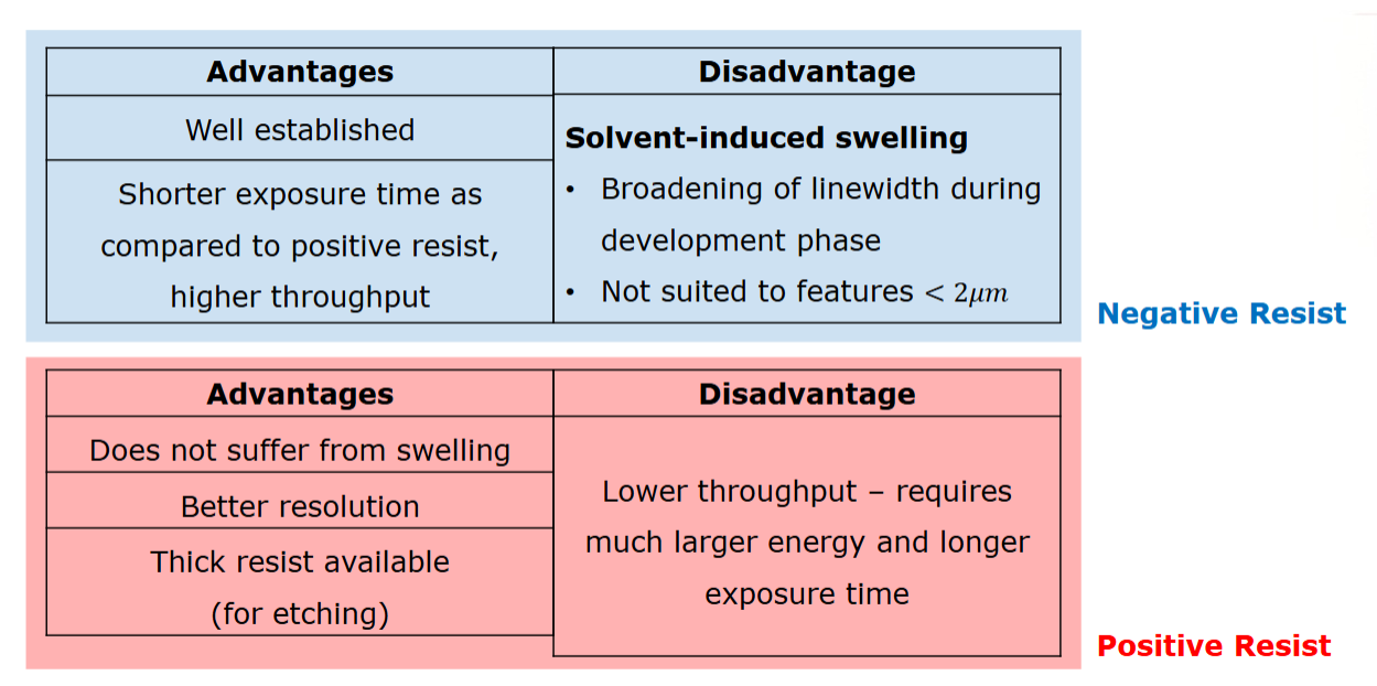
注意:正光刻胶是在光照中被溶解,而负光刻胶是在光照中被固化。
现在工业中更喜欢使用正光刻胶,因为有更好的Resolution。
2.5 Chemically Amplified DUV Resist(化学放大深紫外光刻胶)
关键是CA Chemical Amplify:
DUV makes PAG Photo Acid Generator to generate acid, PEB diffusion acid
2.6 Standing wave effect
解释:Input light reflected and diffusion with reflected light, standing wave formed Zigzag or swing curve
如何减少驻波效应:
① Dye PR more absorption
② PEB flat the zigzag(PEB also helps by smoothing out the zigzag due to resist thermal reflow)
③ ARC anti-reflective